Explain how doping works in semiconductors?
1 Answer

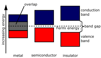
Doping is often encountered when making a semiconductor, such as for diodes and transistors. (I'm not going to explain those as it's outside the scope of the question.) These decrease the band gap for semiconductors, improving conductivity.
An example of this is using a boron dopant to improve the conductivity of a silicon material. Silicon has long flexible bonds, which give a good amount of room for electrons to move.
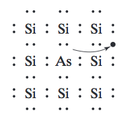
Also, since it is in group 14, it has 4 valence electrons. While bonding in silicon networks, if one empty orbital is available in an inserted dopant, silicon becomes an electron donor.
Boron in contrast is in group 13 and is an electron acceptor, since it has only three valence electrons, all three of which would be used in bonding in a network.
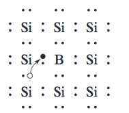
In these silicon networks, if you substitute one silicon for a boron, you have introduced an electron acceptor, improving the electron mobility and making a p-type semiconductor (since you've introduced many holes, which are positively charged).
- A valence electron jumps from one boron atom into that "hole" in the silicon atom's valence shell
- The electron that leaves leaves behind a hole from which it came that other electrons then fill back up
- This cycle continues for as long as boron atoms are still substituting for some of the silicon atoms in the silicon material
This could be done with arsenic (5 valence electrons) instead of boron as well, and you would get an n-type semiconductor since there are more mobile electrons than holes.
Overall, semiconductors don't have a "bridge" between their low- and high-energy bands, so having the dopant acts essentially to decrease the band gap in the context of band theory.